

Image Credit: Associated Press
Listen to the audio version of this article (generated by AI).
Key Points
- Electronic-photonic integration dramatically reduces AI data-center power consumption while boosting speed and bandwidth by combining electronic and photonic chips on a single package and transmitting data with light rather than electricity.
- New optical couplers developed through MIT’s FUTUR-IC program enable AI chips to transfer more than one petabit of data per second, with a roadmap toward 10 petabits per second by 2030.
- Major chipmakers like Nvidia, AMD, Broadcom, Marvell, and others are investing billions in co-packaged optics and photonic technologies, positioning themselves to benefit if MIT’s next-generation chip designs become the new standard for AI infrastructure.
AI data centers consume a massive amount of energy. In fact, they require more energy than traditional power grids can handle right now. We’ve covered that topic quite a bit at MarketWise, including a number of viable alternative energy sources that could reduce reliance on the grid – nuclear, solar, natural gas, and geothermal, to name a few.
But there’s a promising new technology that may actually solve the AI energy crisis being developed by the Massachusetts Institute of Technology (“MIT”) and its FUTUR-IC research program. It’s known as electronic-photonic integration.
How Electronic-Photonic Integration Works
Without getting overly technical, electronic-photonic integration is essentially the efficient integration of both electronic microchips and photonic chips into one component.
This technology uses silicon photonics to drastically increase chip bandwidth while just as substantially reducing energy consumption and heat generation – both of which are major AI data-center bottlenecks.
Silicon-photonics technology uses light rather than electrical signals to transmit and process data at incredibly high speeds. Routing photons through small, modified silicon circuits is how this technology can increase speed while reducing energy use and heat. This is made possible through optical communication, which uses significantly less energy than electrical signals.
The result is what’s called co-packaged optics (“CPO”), a perfect example of electronic-photonic integration.
Santec, a global leader in photonic and optical technologies, describes CPO like this:
Co-packaged optics (CPO) refers to integrating optical transceivers and switching ASICs [application-specific integrated circuits] within a single package. Instead of connecting the switch chip to pluggable optical modules through electrical traces on a printed circuit board (PCB), CPO brings the optics directly adjacent to the chip. This shift significantly reduces the length and complexity of the electrical connections between them.
Manufacturers create CPO by placing photonic integrated circuits (“PICs”) – which transmit information using light – close to compute microchips, such as ASICs or graphics processing units (“GPUs”) – which process information using electricity – on the same silicon wafer. The photonics engines then route light-based data rather than depending only on electrical signals.
Having both components on the same chip minimizes the distance between signals, reducing power consumption and speeding up data transfer.
As AI models become larger and more complex, and cloud services continue to grow, photonic integration looks like a potential game-changer. It could help the tech industry dramatically cut back on the amount of power that data centers need to run AI workloads and cloud computing.
But MIT has even bigger plans for it.
MIT Takes Electronic-Photonic Integration to the Next Level
MIT’s FUTUR-IC research program has taken the science of electronic-photonic integration to another level – one that could forever change the way data centers use energy.
The program has developed two new devices that further simplify electronic-photonic integration – a process that has proven to be quite challenging and expensive.
One is the evanescent coupler, and the other is a graded-index (“GRIN”) coupler, both of which are designed to transfer light more efficiently between photonic devices. More specifically, these couplers will allow next-generation AI chips to transmit more than one petabit of data per second… and use far less power in doing so. (A third coupler, developed by another MIT team, is part of the design as well.)
For context, moving one petabit of data per second would be the equivalent of downloading the entire Netflix library in one second.
When used together, these couplers serve as “optical solder bumps” (rather than literal metal, electrically conductive bumps) that transfer light between photonic components, rather than carrying electrical signals, which consume more energy and incur more resistance and power loss as data rates increase.
Those optical solder bumps are instrumental to how chips are packaged more efficiently together. This physical packaging of chips, according to MIT, “leapfrogs over the current technology barriers to scaling function and speed.”
Speaking of speed… MIT isn’t settling for the blazing-fast data transfer rate of one petabit per second. It’s aiming for roughly 10 petabits per second by 2030.
MIT’s approach to electronic-photonic integration essentially replaces electrical conduction for data transfer and communication with optical light transference. This makes the physical packaging and manufacturing of these AI chips easier and more efficient, while vastly improving data-transfer speed and significantly reducing the energy required.
Perhaps even more impactful, MIT’s researchers determined that this type of chip could be built at scale with existing semiconductor-manufacturing equipment. That is massive. And it pushes up the possible timeline for large-scale production and deployment.
When might that be? Photonic chips are already commercially viable and are being used by some very noteworthy tech players, such as Nvidia (NVDA), Broadcom (AVGO), and Advanced Micro Devices (AMD), to name a few.
But MIT’s iteration is probably a few years away. While MIT’s prototypes have been successful, the ball is in the court of chip manufacturers right now. Because these chips would be manufactured in already-existing foundries – with no change in equipment – those manufacturers need to determine how the chips would be assembled.
To resolve that challenge, MIT’s Microphotonics Center gathered with companies like Nvidia, Meta Platforms (META), and AMD at the institution’s 2026 Spring Meeting to discuss these new chips. But the adoption timeline remains largely unknown.
What we do know is that MIT projects a 10-petabit-per-second chip will be ready by 2030. So, we can reasonably assume that production would begin sometime near the end of the decade.
Major Chipmakers Are Scaling Silicon Photonics. Will a Shortage Follow?
I alluded to the fact that some chipmakers are already investing in photonic technology and implementing it into their chips.
Nvidia, for example, has committed to pouring at least $6.5 billion into companies specializing in photonics. In March 2026 alone, Nvidia invested $2 billion each in Coherent (COHR), Marvell Technology (MRVL), and Lumentum (LITE) while also making multibillion-dollar commitments to purchase silicon photonics and optical interconnection components.
Nvidia also forged a deal to invest up to $3.2 billion in Corning (GLW), with Corning opening three new plants in the U.S., each dedicated solely to manufacturing optical technology for Nvidia.
With Nvidia’s heavy investment in photonics and optical connectivity, it’s fair to wonder whether photonics will soon be in short supply. That’s one reason why the company joined the $500 million funding round for Silicon Valley semiconductor startup Ayar Labs, which specializes in integrating high-speed optical connections directly into AI compute chips.
In June, Ayar Labs joined the Nvidia NVLink Fusion ecosystem to embed CPO directly into next-generation AI infrastructure. By investing in Ayar Labs, Nvidia secures a robust supply chain before the marketplace becomes too crowded.
Unsurprisingly, other significant AI players have joined the optical parade.
AMD acquired PIC startup company Enosemi last May to speed up its CPO production. The company also partnered with GlobalFoundries (GFS) for PIC manufacturing for its upcoming Instinct MI500 series of AI accelerators, scheduled for release next year.
Semiconductor giant Broadcom has already deployed its CPO products and custom ASICs in Meta’s and Alphabet’s (GOOGL) data-center facilities. The company partners with Taiwan Semiconductor Manufacturing (“TSMC”) (TSM), using TSMC’s electronic and photonic circuit integration process. Broadcom also works with Corning to help integrate optical fibers and components into Broadcom’s CPO offerings.
Marvell acquired Polariton Technologies and Celestial AI to expand its components’ bandwidth and architecture. And the company is addressing the chip-capacity and power-usage bottlenecks with its Photonic Fabric platform and 3D silicon-photonics engine, which integrates optics into its chips. In tandem with chip foundry Tower Semiconductor (TSEM), Marvell has shipped more than five million coherent PICs to its customers worldwide.
What MIT’s Photonics Advancements Mean for Investors
There is substantial momentum behind photonic integration across the entire semiconductor industry. Using optical technology to both increase chip bandwidth and decrease power consumption offers a practical solution to the current AI bottlenecks and the AI-driven power crisis.
The fact that MIT’s next-generation electronic-photonic chips could soon be manufactured at scale in existing semiconductor factories is also a potentially huge breakthrough. And it’s one that investors can’t ignore.
Nvidia, Broadcom, AMD, and Marvell have all experienced stock growth over the past year.
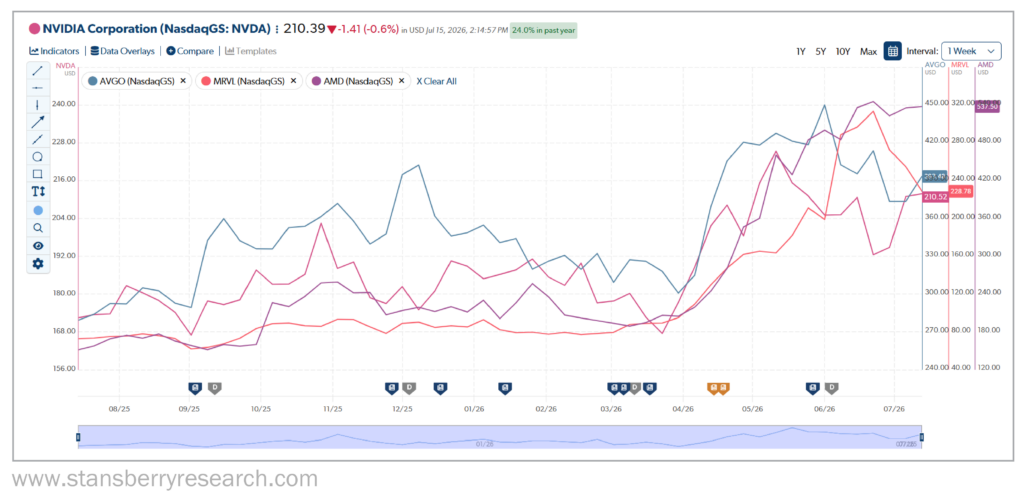
And, assuming these companies eventually adopt MIT’s coupler-equipped chip design and produce it commercially, demand for these stocks could soar beyond their already-astronomical levels.
MIT’s breakthrough technology, if successfully produced at scale, could fundamentally change how AI companies do business while going a long way toward quenching AI’s relentless thirst for power. And that could have a profound impact on every business that manufactures these chips, as well as those integrating them into their data centers and infrastructures.
Editor’s Note: A new “dark energy” is being rolled out as we speak… It completely bypasses our need for foreign oil. And it’s not nuclear or solar or wind or anything you would expect.
This new potential $10 trillion technology is already seeing investment by early backers of Microsoft, Google, Amazon, and more… Most important, these dozens of billionaires can’t make this tech themselves. They have to go through obscure “supplier” companies.
And in the coming months, this new “dark energy” could send three little-known stocks soaring… while wiping out 10 of the most popular stocks on the market. Learn more about this dark energy opportunity by clicking right here.